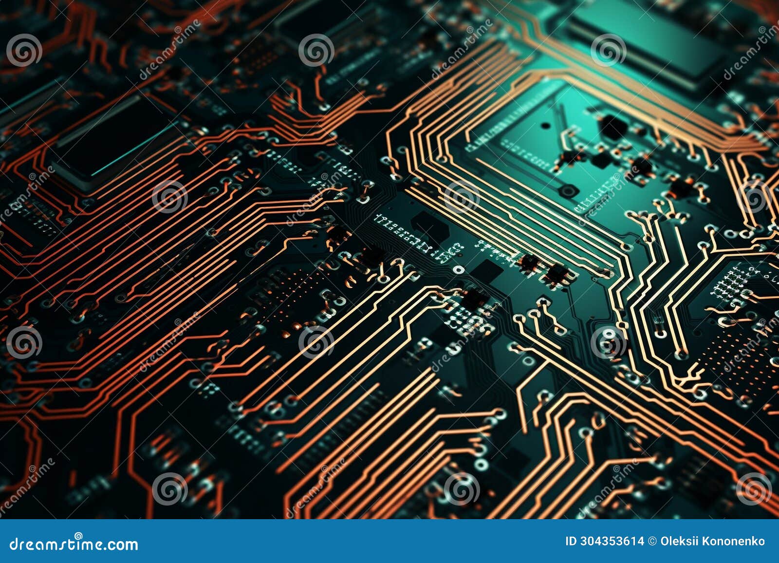
Copper Traces Circuit Board . October 22, 2019 by mark hughes, advanced assembly. however, when a pcb trace—the copper pathways on the board—becomes damaged, it can disrupt the flow of electricity, leading to. the circuit board trace refers to the routing network, fuses, insulation, and copper that make up the pcb. the “trace” component refers to the width of a designated copper pathway, whereas “space” delineates the width of the void separating two. determining copper trace thickness in pcb design. copper traces frequently referred to as “traces” or “tracks,” a pcb copper trace is a thin strip of copper etched onto the board surface. copper traces are an essential component of printed circuit boards (pcbs), providing the pathways for electric current to flow. pcb copper plating—also known as copper coating, copper finish, and surface finish—has two essential.
from www.dreamstime.com
pcb copper plating—also known as copper coating, copper finish, and surface finish—has two essential. copper traces frequently referred to as “traces” or “tracks,” a pcb copper trace is a thin strip of copper etched onto the board surface. October 22, 2019 by mark hughes, advanced assembly. copper traces are an essential component of printed circuit boards (pcbs), providing the pathways for electric current to flow. however, when a pcb trace—the copper pathways on the board—becomes damaged, it can disrupt the flow of electricity, leading to. the circuit board trace refers to the routing network, fuses, insulation, and copper that make up the pcb. determining copper trace thickness in pcb design. the “trace” component refers to the width of a designated copper pathway, whereas “space” delineates the width of the void separating two.
An Advanced Circuit Board with Intricate Gold and Copper Traces, Set on
Copper Traces Circuit Board copper traces are an essential component of printed circuit boards (pcbs), providing the pathways for electric current to flow. pcb copper plating—also known as copper coating, copper finish, and surface finish—has two essential. October 22, 2019 by mark hughes, advanced assembly. the circuit board trace refers to the routing network, fuses, insulation, and copper that make up the pcb. copper traces are an essential component of printed circuit boards (pcbs), providing the pathways for electric current to flow. copper traces frequently referred to as “traces” or “tracks,” a pcb copper trace is a thin strip of copper etched onto the board surface. the “trace” component refers to the width of a designated copper pathway, whereas “space” delineates the width of the void separating two. determining copper trace thickness in pcb design. however, when a pcb trace—the copper pathways on the board—becomes damaged, it can disrupt the flow of electricity, leading to.
From www.dreamstime.com
A Complex Circuit Board Adorned with Gold and Copper Traces on a Dark Copper Traces Circuit Board October 22, 2019 by mark hughes, advanced assembly. however, when a pcb trace—the copper pathways on the board—becomes damaged, it can disrupt the flow of electricity, leading to. pcb copper plating—also known as copper coating, copper finish, and surface finish—has two essential. the “trace” component refers to the width of a designated copper pathway, whereas “space” delineates. Copper Traces Circuit Board.
From yic-assm.com
Why Do We Use Copper to Make PCB Traces? Yun Industrial Copper Traces Circuit Board however, when a pcb trace—the copper pathways on the board—becomes damaged, it can disrupt the flow of electricity, leading to. determining copper trace thickness in pcb design. pcb copper plating—also known as copper coating, copper finish, and surface finish—has two essential. the “trace” component refers to the width of a designated copper pathway, whereas “space” delineates. Copper Traces Circuit Board.
From www.dreamstime.com
An Advanced Circuit Board with Intricate Gold and Copper Traces, Set on Copper Traces Circuit Board the circuit board trace refers to the routing network, fuses, insulation, and copper that make up the pcb. copper traces frequently referred to as “traces” or “tracks,” a pcb copper trace is a thin strip of copper etched onto the board surface. the “trace” component refers to the width of a designated copper pathway, whereas “space” delineates. Copper Traces Circuit Board.
From www.freepik.com
Premium Photo Top view of a detailed circuit board with various Copper Traces Circuit Board copper traces frequently referred to as “traces” or “tracks,” a pcb copper trace is a thin strip of copper etched onto the board surface. the circuit board trace refers to the routing network, fuses, insulation, and copper that make up the pcb. the “trace” component refers to the width of a designated copper pathway, whereas “space” delineates. Copper Traces Circuit Board.
From www.omnicircuitboards.com
What is a Superconducting Circuit Trace? How is it different from a Copper Traces Circuit Board copper traces are an essential component of printed circuit boards (pcbs), providing the pathways for electric current to flow. copper traces frequently referred to as “traces” or “tracks,” a pcb copper trace is a thin strip of copper etched onto the board surface. October 22, 2019 by mark hughes, advanced assembly. determining copper trace thickness in pcb. Copper Traces Circuit Board.
From huiwenedn.com
What PCB Copper Thickness Should You Use? Blog CircuitMaker Copper Traces Circuit Board determining copper trace thickness in pcb design. the “trace” component refers to the width of a designated copper pathway, whereas “space” delineates the width of the void separating two. pcb copper plating—also known as copper coating, copper finish, and surface finish—has two essential. however, when a pcb trace—the copper pathways on the board—becomes damaged, it can. Copper Traces Circuit Board.
From www.freepik.com
Premium Photo Macro shot of a diode bridge rectifier on a green Copper Traces Circuit Board copper traces are an essential component of printed circuit boards (pcbs), providing the pathways for electric current to flow. copper traces frequently referred to as “traces” or “tracks,” a pcb copper trace is a thin strip of copper etched onto the board surface. October 22, 2019 by mark hughes, advanced assembly. pcb copper plating—also known as copper. Copper Traces Circuit Board.
From camptechii.com
18 PCB Layout Tips for Improving Your PCB Design and Reducing Copper Traces Circuit Board determining copper trace thickness in pcb design. the “trace” component refers to the width of a designated copper pathway, whereas “space” delineates the width of the void separating two. pcb copper plating—also known as copper coating, copper finish, and surface finish—has two essential. however, when a pcb trace—the copper pathways on the board—becomes damaged, it can. Copper Traces Circuit Board.
From www.alamy.com
A green circuit board with copper traces. There are no components on Copper Traces Circuit Board copper traces frequently referred to as “traces” or “tracks,” a pcb copper trace is a thin strip of copper etched onto the board surface. pcb copper plating—also known as copper coating, copper finish, and surface finish—has two essential. October 22, 2019 by mark hughes, advanced assembly. copper traces are an essential component of printed circuit boards (pcbs),. Copper Traces Circuit Board.
From www.pinterest.ca
Heavy copper printed circuit board Copper print, Printed circuit Copper Traces Circuit Board copper traces frequently referred to as “traces” or “tracks,” a pcb copper trace is a thin strip of copper etched onto the board surface. determining copper trace thickness in pcb design. copper traces are an essential component of printed circuit boards (pcbs), providing the pathways for electric current to flow. the circuit board trace refers to. Copper Traces Circuit Board.
From www.reddit.com
Why are the copper traces on this computer motherboard so wavy? r Copper Traces Circuit Board the circuit board trace refers to the routing network, fuses, insulation, and copper that make up the pcb. copper traces frequently referred to as “traces” or “tracks,” a pcb copper trace is a thin strip of copper etched onto the board surface. the “trace” component refers to the width of a designated copper pathway, whereas “space” delineates. Copper Traces Circuit Board.
From www.reddit.com
A PCB with the copper traces exposed r/EngineeringPorn Copper Traces Circuit Board the circuit board trace refers to the routing network, fuses, insulation, and copper that make up the pcb. pcb copper plating—also known as copper coating, copper finish, and surface finish—has two essential. October 22, 2019 by mark hughes, advanced assembly. copper traces frequently referred to as “traces” or “tracks,” a pcb copper trace is a thin strip. Copper Traces Circuit Board.
From www.ourpcb.com
Controlled Impedance PCB PCB Copper Traces with Minimal Signal Copper Traces Circuit Board the circuit board trace refers to the routing network, fuses, insulation, and copper that make up the pcb. pcb copper plating—also known as copper coating, copper finish, and surface finish—has two essential. copper traces frequently referred to as “traces” or “tracks,” a pcb copper trace is a thin strip of copper etched onto the board surface. . Copper Traces Circuit Board.
From www.royalcircuits.com
Copper Trace and Space Three Factors to Consider Royal Circuits Copper Traces Circuit Board determining copper trace thickness in pcb design. the circuit board trace refers to the routing network, fuses, insulation, and copper that make up the pcb. pcb copper plating—also known as copper coating, copper finish, and surface finish—has two essential. however, when a pcb trace—the copper pathways on the board—becomes damaged, it can disrupt the flow of. Copper Traces Circuit Board.
From www.dreamstime.com
Green Circuit Board with Copper Traces and Electronic Components Copper Traces Circuit Board determining copper trace thickness in pcb design. copper traces are an essential component of printed circuit boards (pcbs), providing the pathways for electric current to flow. the “trace” component refers to the width of a designated copper pathway, whereas “space” delineates the width of the void separating two. October 22, 2019 by mark hughes, advanced assembly. . Copper Traces Circuit Board.
From www.raypcb.com
Relationship between PCB Copper Weight, Trace Width and Current Copper Traces Circuit Board determining copper trace thickness in pcb design. October 22, 2019 by mark hughes, advanced assembly. however, when a pcb trace—the copper pathways on the board—becomes damaged, it can disrupt the flow of electricity, leading to. the “trace” component refers to the width of a designated copper pathway, whereas “space” delineates the width of the void separating two.. Copper Traces Circuit Board.
From www.pcba-manufacturers.com
A complete guide on PCB copper trace PCBA Manufacturers Copper Traces Circuit Board pcb copper plating—also known as copper coating, copper finish, and surface finish—has two essential. October 22, 2019 by mark hughes, advanced assembly. determining copper trace thickness in pcb design. copper traces are an essential component of printed circuit boards (pcbs), providing the pathways for electric current to flow. the circuit board trace refers to the routing. Copper Traces Circuit Board.
From www.pcba-manufacturers.com
A complete guide on PCB copper trace PCBA Manufacturers Copper Traces Circuit Board determining copper trace thickness in pcb design. copper traces are an essential component of printed circuit boards (pcbs), providing the pathways for electric current to flow. copper traces frequently referred to as “traces” or “tracks,” a pcb copper trace is a thin strip of copper etched onto the board surface. pcb copper plating—also known as copper. Copper Traces Circuit Board.